NANOscientific
Forum Europe 2026
09 - 11 September, 2026 | Charles University, Prague, Czech Republic
The 9th edition of the NANOscientific Forum Europe will be held at the Faculty of Mathematics and Physics, Charles University, Prague, Czech Republic from September 09 – 11, 2026. Our host will be Dr. Martin Rejhon, a group leader at the Institute of Physics at Charles University, and renowned for his work on epitaxial graphene on silicon carbide. He will be supported by Dr. Shirly Espinoza from ELI Beamlines as his co-host.
Why attend NSFE2026?
The NSFE2026 brings together scientists, engineers, students, and industry professionals working in materials science, life sciences, and surface analysis.
The forum offers:
• 🧠 Expert talks from leading researchers
• 🔬 Hands-on sessions with state-of-the-art instruments
• 🤝 Networking opportunities with peers and innovators
The NSFE2026 will spotlight the latest advances in nanotechnology, with focus sessions on 2D Materials and Imaging Spectroscopic Ellipsometry. Further topics will include bio applications, advanced techniques, electrochemistry, and surface and thin film metrology. Attendees will gain insights into both fundamental research and applied techniques across materials and life sciences.
Another highlight of the event will be live demonstrations of cutting-edge instrumentation, including:
• Park FX40 AFM
• Park NX10 AFM
• Park NX20 AFM with sMIM
• Park NX1 AFM
• Accurion EP4 Imaging Spectroscopic Ellipsometer
• Lyncée Digital Holographic Microscope
These sessions offer hands-on experience with tools that enable high-resolution imaging, electrical and magnetic property mapping, and advanced optical characterization. Applications will span nano imaging, advanced materials, and semiconductors. And as in previous years the event will extend beyond scientific discussions and offer participants many opportunities to network in a more relaxed setting—with more details to follow soon.
- Session 1: Graphene and 2D Materials at the Nanoscale
- Session 2: Biointerfaces, Cells and Nanoscale Mechanics
- Hands-on Session
- Poster Session
- Conference Dinner
FULL DAY (08:30 - 22:00, CEST)
- Session 3: Nanoscale Interface Metrology for Energy, Electronics and Molecular Materials
- Session 4: Imaging Ellipsometry and Optical Thin-Film Metrology
- Hands-on Session
- Social Activity
FULL DAY (08:30 - 22:00, CEST)
- Session 5: Frontiers in AFM, SPM and Nanoscale Metrology
HALF DAY (08:30 - 14:00, CEST)
- Deadline Contributed Abstract: 15. June
- Deadline Poster Abstract: 31. August
- Early Bird Registration: 31. May
- Standard Registration: 31. August
Registration & Meet and Greet
Welcome to the NSFE2026
Intro Session 1: Graphene and 2D Materials at the Nanoscale
Keynote Talk: Electrical AFM modes for investigating ABC-stacked graphene domains in epitaxial graphene
Electrical AFM modes for investigating ABC-stacked graphene domains in epitaxial graphene
In graphene, emergent properties ranging from superconductivity to ferroelectricity have been observed in ABC-stacked domains. These domains are typically obtained through exfoliation followed by expert mechanical twisting and alignment to the desired orientation, a process that is highly challenging and not scalable.
Here, we demonstrate that ABC-stacked graphene domains can be obtained using a scalable growth technique, namely the thermal decomposition of silicon carbide. Using conductive atomic force microscopy (c-AFM), we identified distinct conductivity patterns in untwisted trilayer epitaxial graphene grown on silicon carbide. These patterns revealed the presence of both ABA and ABC domains (Fig. 1a), consistent with the conductivity differences observed in twisted exfoliated graphene and predicted by density functional theory. Similar patterns were also observed using scanning microwave impedance microscopy (sMIM), which revealed distinct resistance (Fig. 1b) and capacitance (Fig. 1c) signatures for ABA and ABC stackings (Fig. 1b) arising from their different electronic band structures.
We further demonstrate that these moiré patterns are driven by strain present in the graphene system, allowing us to control the domain size by tuning the strain (Fig. 1a). This finding opens the way for future electronic and optoelectronic applications requiring large-area ABC-stacked graphene domains.
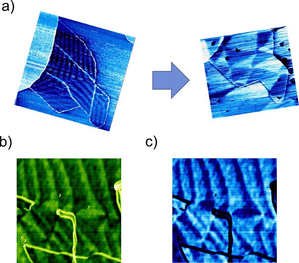
Figure 1 a)c-AFM image of an epitaxial graphene film with visible stripes in conductivity on a three layeref epitaxial graphene and change in Moire pattern after strain engineering. b) Resistance and c) capacitance signal from sMIM measurement.

Keynote Talk: Title tbc

Keynote Talk: Fabricating, Probing, and Sliding vdW Polytypes with an AFM Tip
Fabricating, Probing, and Sliding vdW Polytypes with an AFM Tip
The field of "Slidtronics" opens exciting opportunities to probe and utilize the physics of atoms and electrons in vdW structures. Today, we can switch one crystalline stacking configuration, "Polytype" to another using only electric fields, providing fascinating multi-ferroic responses at <fJ switching energies and <ns switching times. The talk will focus on crucial experimental steps enabled by KPFM measurements and AFM lithography, spanning from our 2020 paper (https://arxiv.org/abs/2010.05182 - introducing the superlubric "SlideTronics" dislocation concept) to a novel sliding ferroelectric resonant tunnel junction (SFeRT) array (https://arxiv.org/abs/2603.00817).

Coffee Break
Contributed Talk: Strain Relaxation Effects in Trilayer Epitaxial Graphene
Strain Relaxation Effects in Trilayer Epitaxial Graphene
Rhombohedral (ABC) stacking in trilayer epitaxial graphene provides superior electronic properties compared to Bernal (ABA) stacking [1–4], making stacking control a key objective in multilayer graphene engineering. Using conductive AFM, ABC and ABA domains can be spatially resolved in as-grown trilayer graphene as regions of low and high local conductivity, respectively, manifesting as stripe-shaped current modulations (Fig. 1(b), (d), (f)). Hydrogen intercalation converts as-grown into Quasi-Free-Standing (QFS) trilayer graphene, releasing the compressive strain, which results in the modification of ABC and ABA domains modulation (Fig. 1(a)). Three distinct strain relaxation regimes are identified: in the High relaxation regime (relaxation > 55%), c-AFM images show no discernible domain patterns (Fig. 1(c)); the Intermediate relaxation regime (55..35% relaxation) exhibits triangular features of varying shape and symmetry (Fig. 1(e)); and the Low relaxation regime (< 35% relaxation) retains stripe-like patterns (Fig. 1(g)). Approximately 50% of all analyzed locations fall within the Intermediate regime. These results demonstrate that stacking order in trilayer graphene can be systematically controlled through strain relaxation engineering.
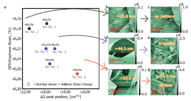
Figure 1: (a) Strain in QFS-three-layer graphene as a function of the ΔG peak position for all analyzed locations, with data color-coded by strain relaxation regime: High, Intermediate, and Low. Color-coded arrows mark the data points corresponding to the representative c-AFM images in panels (b–g); the relative strain change is indicated above each selected point. Panels (b,c), (d,e), and (f,g) show representative c-AFM images of as-grown and QFS-three-layer graphene in the High, Intermediate, and Low strain relaxation regimes, respectively.
-
References
[1] Katsuaki Sugawara, Norifumi Yamamura, Keita Matsuda,Wataru Norimatsu, Michiko Kusunoki, Takafumi Sato, and Takashi Takahashi. Selective fabrication of free-standing aba and abc trilayer graphene with/without dirac-cone energy bands. NPG Asia Materials, 10(2):e466–e466, February 2018.
[2] Debora Pierucci, Thomas Brumme, Jean-Christophe Girard, Matteo Calandra, Mathieu G. Silly, Fausto Sirotti, Antoine Barbier, Francesco Mauri, and Abdelkarim Ouerghi. Atomic and electronic structure of trilayer graphene/sic(0001): Evidence of strong dependence on stacking sequence and charge transfer. Scientific Reports, 6(1), 2016.
[3] Tymofiy Khodkov, Ivan Khrapach, Monica Felicia Craciun, and Saverio Russo. Direct observation of a gate tunable band gap in electrical transport in abc-trilayer graphene. Nano Letters, 15(7):4429–4433, 2015.
[4] Debora Pierucci, Haikel Sediri, Mahdi Hajlaoui, Jean-Christophe Girard, Thomas Brumme, Matteo Calandra, Emilio Velez-Fort, Gilles Patriarche, Mathieu G. Silly, Gabriel Ferro, V´eronique Souli`ere, Massimiliano Marangolo, Fausto Sirotti, Francesco Mauri, and Abdelkarim Ouerghi. Evidence for flat bands near the fermi level in epitaxial rhombohedral multilayer graphene. ACS Nano, 9(5):5432–5439, April 2015.

Contributed Talk: Substrate interaction on the local exciton/trion ratio in mono- to few-layer WS2
Substrate interaction on local exciton/trion ratio in mono- to few-layer WS₂
Appanna Parvangada1,2, Dmitrii Sychev1, Ilka Hermes1
1Leibniz Institute of Polymer Research Dresden e.V., Hohe Str. 6, 01069 Dresden, Germany
2Institute of Applied Physics, Dresden University of Technology, Nöthnitzer Straße 61, 01187 Dresden, Germany
Semiconducting two-dimensional (2D) tungsten disulfide (WS₂) due to its high photoluminescence yield, tunable bandgap, quantum confinement, large exciton binding energy, strong light-matter interaction, along with its low dimensionality and flexibility is a promising candidate for various lightweight optoelectronic devices like light-emitting diodes (LEDs), solar cells and photodetectors.
However, the implementation of 2D materials for large-scale application is often hindered owing to their high spatial heterogeneity due to variation in layer thickness, substrate interaction and local strain on the nanoscale. Therefore, standard optical characterization methods like Photoluminescence (PL) and Raman spectroscopy, which commonly provide such information, can lack the spatial resolution to resolve these variations. Hence, we employ electrical atomic force microscopy (AFM) with in-situ illumination to gain the information regarding the impact of layer thickness, changes in substrate interactions and local strain on the material’s optoelectronic response on the nanoscale.
Within our study, the capabilities of photo-Kelvin probe force microscopy (pKPFM) to capture local photo-potential in mono and few-layer WS2 is demonstrated and the results are correlated to PL spectroscopy. Additionally, the nature (metal or semiconductor) of the substrate and the influence of the work function on the local charge carriers was investigated.

Contributed Talk: Scaling trend, critical length and thickness strain dependence of elastic properties of atomically thin 2H-MOS2 films
SCALING TREND, CRITICAL LENGTH AND THICKNESS STRAIN DEPENDENCE OF ELASTIC PROPERTIES OF ATOMICALLY THIN 2H-MOS2 FILMS
Kalaiarasan Meganathan1,2, Senthil Kumar Eswaran2, Zdeněk Sofer1
1 Department of Inorganic Chemistry, University of Chemistry and Technology, Prague
2 2DML, Department of Physics and Nanotechnology, SRM Institute of Science and Technology, Chennai.
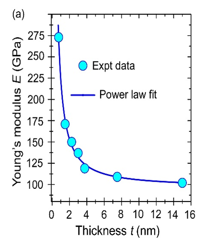
Next-generation flexible electronics require a deep understanding of the mechanical limits of 2D semiconductors to ensure their effective use in strain-engineered devices. Herein, we investigate the elastic scaling behavior of gas-phase CVD-grown atomically-thin 2H-MoS2 films for various thickness 0.75–15 nm. Mechanical crossover at a critical thickness tc ~3.0 nm has found, below which nanoscale elastic-size effects dominate, defining a true-2D regime, while thicker films (t > tc) exhibit bulk-like behavior. The Young’s modulus scales with thickness as E ∝ t−1.16, whereas the bending modulus follows D ∝ t2.91, marking a transition from atomically-flexible to a rigid-regime for t > tc. Monolayer MoS2 exhibit a maximum elastic strain energy of 1.55 J/cm², arising from strong in-plane strain induced by van der Waals epitaxial coupling. These results offer essential mechanical benchmarks for guiding the design of strain-engineered, flexible MoS2 devices.

Contributed Talk: Enhanced interlayer shear locking in Rhomohedral Graphene
ENHANCED INTERLAYER SHEAR LOCKING IN RHOMOHEDRAL GRAPHENE
Wujoon Cha1, Lorenzo Schellack1, Jin Wang2, Mykhailo Shestopalov3, Jan Kunc3, Martin Rejhon3, Erio Tosatti2, Elisa Riedo1
1New York University, Brooklyn, NY 11201, United States of America
2Internation School for Advanced Studies, Trieste, 34151, Italy
3Charles University, Prague, 12116, Czech Republic
Rhombohedral (ABC) graphene has emerged as one of the most promising platforms for correlated quantum phenomena, including superconductivity, magnetism, and strongly correlated electronic phases [1]. In contrast to the more common Bernal (ABA) stacking, these exotic states are uniquely associated with the rhombohedral structure and are believed to be influenced by enhanced interlayer coupling. Raman spectroscopy studies have shown that ABA and ABC graphene exhibit distinct interlayer shear phonons [2,3], indicating differences in the forces that govern relative sliding between neighboring layers. The interfacial transverse shear modulus quantifies the resistance of adjacent graphene layers to relative sliding and is therefore a direct measure of the strength of interlayer mechanical coupling [4]. Because the frequencies of interlayer shear phonons are determined by the same restoring forces, measuring the shear modulus provides a quantitative probe of stacking-dependent lattice dynamics and interlayer interactions that may influence the unique electronic properties of rhombohedral graphene. Despite its importance, direct measurements of the transverse shear modulus in ABC graphene have remained challenging. Mechanical properties associated with interlayer motion are particularly difficult to probe in atomically thin materials because they originate from weak van der Waals interactions and involve deformations spanning only a few atomic layers. Thus, quantitative experimental studies of stacking-dependent interlayer shear stiffness in rhombohedral graphene have remained largely unexplored.
Here, we employ modulated nanoshear force microscopy (MoNS) to directly measure the transverse shear modulus of ABA- and ABC-stacked three-layer epitaxial graphene grown on SiC. A custom automated measurement platform enables statistically significant shear mapping with sub-10 nm spatial resolution across hundreds of locations. The naturally occurring ABA and ABC domains in epitaxial graphene provide a unique opportunity to compare the mechanical response of the two stacking configurations within a single sample. The measurements reveal a clear stacking-dependent contrast, with ABC graphene exhibiting an average transverse shear modulus of approximately 3.5 GPa compared to 2.6 GPa for ABA graphene, corresponding to an enhancement of about 25%. Spatial mapping demonstrates a direct correlation between the measured shear modulus and the underlying stacking domains identified by conductive atomic force microscopy. Density functional theory and molecular dynamics simulations independently reproduce the enhanced shear stiffness of ABC graphene and further reveal a pronounced directional dependence of shear response that is absent in ABA stacking. These results provide the direct experimental evidence of enhanced interlayer shear locking in rhombohedral graphene. More broadly, they establish nanoscale shear mapping as a powerful approach for probing stacking-dependent mechanical coupling in layered materials and provide quantitative insight into a fundamental structural parameter that may contribute to the unique quantum behavior of rhombohedral graphene.
[1] Zhou et al., Nat. 598, 434 (2201)
[2] Lui et al., Appl. Phys. Lett. 106, 041904 (2015)
[3] Tan et al., Nat. Mater., 11, 294 (2012)
[4] Rejhon et al., Nat. Nanotechnol., 17, 1280 (2022)

Intro Session 2: Biointerfaces, Cells and Nanoscale Mechanics
Keynote Talk: The Atomic Force Microscopy cantilever: a multimodal platform to decipher mechanics, nanomotion, and communication in living systems
The Atomic Force Microscopy cantilever: a multimodal platform to decipher mechanics, nanomotion, and communication in living systems
Atomic Force Microscopy (AFM) has transcended its original role as a high-resolution topographical imaging tool to become a highly versatile, multimodal platform for investigating single-cell and cluster-level biophysics. This presentation explores the unique capabilities of the AFM cantilever as a nanoscale sensor to evaluate the morphology, ultrastructure, and nanomechanical properties of living biological systems in real time. By correlating AFM with optical and fluorescence microscopy and with spectroscopy, we achieve a comprehensive, multidimensional overview of cellular dynamics. Thus, we will show how a correlative approach, coupling membrane roughness, Young's modulus and confocal microscopy, unveils the complex structural and nanomechanical alterations occurring during the oxidative aging of red blood cells, linking nanoscale cytoskeletal instability to metabolic degradation and vesicle formation.
Furthermore, the AFM cantilever acts as a highly sensitive, stand-alone nanomechanical oscillator, a nanomotion sensor which can transduce the minute, metabolic vibrations of specimens into measurable signals, offering a real-time signature of life. We will discuss the profound clinical utility of nanomotion sensing in executing rapid antibiotic susceptibility testing (AST) on bacterial species like Escherichia coli and Staphylococcus aureus .
Beyond these applications, the sensitivity to acoustic-like fluctuations opens new avenues for using cantilever sensors to understand complex cell behaviors. Recent findings reveal how clusters of neuroblastoma cells utilize acoustic mechanical waves for long distance cell-cell communication which could trigger mechanotransduction cascades that alter metabolic activity. Ultimately, these pioneering, cantilever-based methodologies are bridging the gap between fundamental biophysics, nanomedicine, and advanced clinical diagnostics.
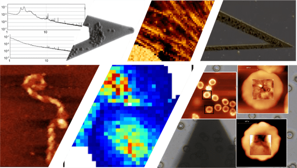
The AFM cantilever as a multimodal platform to study different aspects of biological systems

Keynote Talk: Engineering of Cellular Microenvironments: Biomechanics and Precision Models for Chronic Disease Research
Engineering of Cellular Microenvironments: Biomechanics and Precision Models for Chronic Disease Research
Chronic inflammatory diseases such as rheumatoid arthritis and inflammatory bowel disease arise from complex interactions between cells and the surrounding microenvironment. While molecular mechanisms have been extensively investigated, the contribution of tissue mechanics to disease progression remains less understood. Recent advances in quantitative biophysical methods have enabled the investigation of cellular responses to mechanical and physicochemical perturbations through label-free measurements of cell mass dynamics using Digital Holographic Microscopy (DHM).(1) Combined with multimodal characterization approaches, including second harmonic generation imaging, Brillouin microscopy, and nanoindentation, these techniques provide detailed information on extracellular matrix organization, tissue mechanics, and disease-associated remodeling. At the same time, advances in biofabrication have expanded the ability to engineer cellular microenvironments with mechanical properties similar to the original tissues of the patients. Precise control of mechanical cues can be achieved through two-photon polymerization of three-dimensional microstructures(2) and through dynamically tunable biomaterials that regulate cell adhesion and mechanosensing(3). Together, quantitative biomechanics, advanced imaging, and precision bioengineering provide powerful tools for developing improved experimental models to investigate how physical cues regulate cellular behavior in health and disease.
References:
1. Colombo F, Villiou M, Taheri F, Fröhlich L, Taale M, Albert V, et al. Fluctuations of Dry and Total Mass of Cells Exposed to Different Molecular Weights of Polyethylene Glycol. Adv Nanobiomed Res. 2023 Apr 15. doi:10.1002/anbr.202200156
2. Colombo F, Taale M, Taheri F, Villiou M, Debatin T, Dulatahu G, et al. Two‐Photon Laser Printing to Mechanically Stimulate Multicellular Systems in 3D. Adv Funct Mater. 2024 Mar 4. doi:10.1002/adfm.202303601
3. Scott S, Villiou M, Colombo F, la Cruz‐García A De, Tydecks L, Toelke L, et al. Dynamic and Reversible Tuning of Hydrogel Viscoelasticity by Transient Polymer Interactions for Controlling Cell Adhesion. Advanced Materials. 2025 Feb 11.
doi:10.1002/adma.202408616

Lunch
Keynote Talk: Advanced Nanofabrication Strategies for Electrochemical/ECL sensing Platforms and Functional Biointerfaces
Advanced Nanofabrication Strategies for Electrochemical/ECL sensing Platforms and Functional Biointerfaces
Nanofabrication represents not merely a means of reducing feature size, but a powerful strategy for the precise engineering of analytical and biological interfaces, with direct implications for both sensing performance and the development of physiologically relevant model systems. In this framework, thermal nanoimprint lithography, electron-beam lithography, and thermal scanning probe lithography are employed for the fabrication of nanoelectrode arrays, multiplexed electrochemiluminescence (ECL) platforms, and large-area tissue-mimetic replicas with sub-15 nm resolution. Such nanoscale control enables the rational design of functional interfaces exhibiting ultrasensitive electrochemical response, geometry-dependent modulation of ECL emission, and high-resolution ECL imaging capabilities [1]. In parallel, complementary bio-nanofabrication approaches afford reusable quasi-three-dimensional replicas and UV-tunable ultrathin polymeric films with bone-mimetic stiffness, providing effective platforms for the modulation of stem cell adhesion and differentiation [2-3]. Collectively, these nanofabrication strategies establish a versatile technological framework for the realization of advanced sensing platforms and functional biointerfaces, while offering new opportunities for the in vitro reproduction of physiologically relevant microenvironments.
References:
[1] C. Mariani, A. Fracassa, P. Pastore, S. Bogialli, F. Paolucci, G. Valenti, A. Zanut*, Chemical & Biomedical Imaging 2025 3 (7), 462-469, DOI: 10.1021/cbmi.5c00022
[2] X. Liu, A. Zanut (first co-author), M. Sladkova-Faure, L. Xiea, M. Weck, X. Zheng, E. Riedo, G. M. de Peppo, Adv. Func. Mat. 2021, 31, 20088662. https://doi.org/10.1002/adfm.202008662. Cover Article.
[3] A. Zanut, R. Li, R. Deng, X. Liu, M. Rejhon, W. Chen, M. Weck, G. M. de Peppo*, E. Riedo*, Advance Healthcare Materials 2022.

Contributed Talk: Mechanical properties of the cell membrane interacting with nanoparticles studied with AFM

Contributed Talk: AI-Driven Quality Assessment and Multi-Model Analysis of AFM Force Curves
AI-Driven Quality Assessment and Multi-Model Analysis of AFM Force Curves
Mathieu COGNARD, Digital Surf, Besançon, France
Force spectroscopy has become an essential tool for probing the nanomechanical properties of polymers and soft matter. It enables the extraction of parameters such as Young’s modulus and adhesion energy at the nanoscale, which are crucial for understanding local structure–property relationships.
However, despite its widespread use, force curve analysis remains a major challenge. Data processing typically requires labor-intensive preprocessing, manual model selection, and curve fitting, often leading to inconsistent results across users and laboratories. Moreover, the coexistence of multiple contact mechanics models—such as Hertz, JKR, and DMT—creates additional ambiguity, especially in heterogeneous or adhesive systems where the choice of model significantly impacts the calculated physical values.
The Tabor coefficient provides a theoretical framework to bridge these models by defining the transition between different adhesion regimes. Yet, this parameter has rarely been implemented in practical analysis tools accessible to experimentalists.
We present new software developments in Mountains® that integrate the Tabor coefficient as an objective criterion to guide model selection automatically. The workflow combines automated preprocessing, simultaneous fitting to several models, and quantitative scoring to identify the most appropriate mechanical description. This approach reduces user bias, improves reproducibility, and enables the reliable treatment of large datasets.
Validation on copolymers and polymer blends demonstrates the robustness of the method. These systems, characterized by local variations in stiffness and adhesion, provide stringent test cases where conventional single-model approaches often fail. In addition to model selection, we introduce an AI-based tool for automated quality assessment. This tool compares acquired curves against a curated reference database, providing real-time feedback on measurement reliability.
Together, these developments establish a comprehensive workflow for AFM nanomechanics, combining physical insight, algorithmic robustness, and artificial intelligence. This methodology paves the way towards standardized and reproducible force curve analysis, offering a scalable framework adaptable to diverse materials and experimental conditions.
Biography of presenting author

Mathieu Cognard is the Product Manager for Scanning Probe Microscopy (SPM) at Digital Surf, France. As a specialist in surface metrology and image analysis, he oversees the strategic development of the Mountains® software family. His role is to bridge the gap between complex instrumental techniques and user-centric software solutions, ensuring that academic and industrial needs are translated into robust analytical tools.
While managing the entire SPM product lifecycle, he specifically focuses on enhancing data reliability through automated workflows and AI-driven quality assessment. His current work on standardizing nanomechanical analysis through multi-model fitting illustrates his commitment to improving reproducibility and quantitative accuracy across diverse material science applications.
Other Details:
Presentation Category: Oral
Email: mcognard@digitalsurf.com
LinkedIn: https://www.linkedin.com/in/mathieu-cognard-26893358/

Contributed Talk: A role for acoustic field in neuron-neuron recognition and interaction
A role for acoustic field in neuron-neuron recognition and interaction
Nanoscale motility of cells is a fundamental phenomenon, closely associated with biological status and response to environmental solicitations, whose investigation has disclosed new perspectives for the comprehension of cell behaviour and fate. To investigate intracellular interactions, we designed an experiment to monitor movements of clusters of neuroblastoma cells (SH-SY5Y) growing on a nanomechanical oscillator (nanomotion sensor) suspended few hundreds of microns over the surface of a Petri dish where other neuroblastoma cells are freely moving. We observed that the free-to-move cells feel the presence of cells on the nearby nanosensor and, simultaneously, the cells on the sensor enhance their motion when clusters of freely moving cells approach. Our observations suggest the presence of additional physical mechanisms, other than the chemical one, and we hypothesize that the acoustic field generated by cell vibrations can have a role in the recognition and interaction between distant clusters. Moreover, we investigated the characteristic of the signal generated by vibrating neurons on the cantilever and we detected the occurrence of low-frequency mechanical rhythms that could be the fingerprint of specific neuronal activities.

Contributed Talk: Liquid-Phase Kelvin Probe Force Microscopy for Mapping Biomolecular Electrostatics at Biosensing Interfaces
Liquid-Phase Kelvin Probe Force Microscopy for Mapping Biomolecular Electrostatics at Biosensing Interfaces
C. Di Franco1, B. J. Rodriguez2, Q. Zhang2, M. Piscitelli3, E. Macchia4, L. Torsi5, G. Scamarcio6
1Consiglio Nazionale delle Ricerche – Istituto di Fotonica e Nanotecnologia, CNR-IFN Bari, Italy
2School of Physics, Conway Institute, University College Dublin, Dublin, Ireland
3Dipartimento Interateneo di Fisica, Università degli Studi di Bari Aldo Moro, Bari, Italy
4Dipartimento di Farmacia-Scienze del Farmaco, Università degli Studi di Bari Aldo Moro, Bari, Italy
5Dipartimento di Chimica, Università degli Studi di Bari Aldo Moro, Bari, Italy
6Consiglio Nazionale delle Ricerche – Istituto Nanoscienze CNR-NANO, NEST-Scuola Normale Superiore, Pisa, Italy
Electrostatic interactions at biofunctional interfaces are central to biomolecular recognition and to the signal amplification mechanisms exploited in label-free biosensors. Kelvin probe force microscopy has emerged as a powerful nanoscale method to correlate surface potential, work-function variations and molecular organization at antibody-functionalized interfaces. In our recent work, KPFM was used to investigate patterned large-area biofunctionalized surfaces for ultrasensitive immunoglobulin detection, providing insight into the reliability of surface-potential mapping for single-binding-event biosensing. In related studies, extended work-function shifts over large-area antibody layers were shown to be triggered by highly specific biomolecular recognition, supporting the concept that single binding events can induce collective electrostatic rearrangements across densely packed biolayers1-3. A major challenge, however, is to extend KPFM from ambient conditions to liquid environments, where biomolecular recognition actually occurs. Conventional closed-loop KPFM is limited in aqueous media by electrochemical phenomena induced by the applied DC bias, including charge screening, Faradaic processes and electrolysis. Open-loop and dual-harmonic KPFM approaches have provided a route to quantitative electrostatic measurements at solid–liquid interfaces, including contact-potential-difference imaging at the graphene–liquid interface and broader nanoscale electrical measurements in liquids4,5. Here, we report the application of dual-harmonic KPFM to model biomolecular interfaces based on patterned Au/anti-IgM substrates. The platform consists of a binary patterned gold and physisorbed anti-IgM regions, providing a controlled interface between bare metal and antibody layer. In air, dual-harmonic KPFM yielded a contact potential difference (CDP) of (249 ± 11) mV between the Au and anti-IgM regions, in close agreement with conventional closed-loop KPFM values of (256 ± 11) mV obtained on the same type of patterned interface. In Milli-Q water environment, DH-KPFM revealed a reversal of the CPD contrast at the Au/anti-IgM interface, suggesting that hydration-induced counterion adsorption and Stern-layer formation strongly affect the electrostatic property distribution of the protein layer.
References
- C. Di Franco et al., Journal of Materials Chemistry C, 2024.
- C. Di Franco et al, Advanced Materials Interfaces, 2023.
- M. Piscitelli, Small Methods, 2025.
- L. Collins, Applied Physics Letters, 2014.
- L. Collins, Beilstein Journal of Nanotechnology, 2015.

Wrap Up Day 1
Coffee Break
Hands-On Sessions
Poster Session
Break
Conference Dinner
Welcome & Intro Session 3: Nanoscale Interface Metrology for Energy, Electronics and Molecular Materials
Keynote Talk: Electrochemical Strain and Strain Waves in Mixed Ionic–Electronic Conductors
Electrochemical Strain and Strain Waves in Mixed Ionic–Electronic Conductors
Materials exhibiting mixed ionic–electronic conductivity play a central role in emerging technologies, including energy storage, bioelectronic interfaces, and neuromorphic computing. In this talk, I will discuss advanced atomic force microscopy (AFM) techniques for probing coupled ionic and electronic transport processes in these materials under operando conditions.
A key phenomenon in mixed conductors is the generation of local electrochemical strain arising from changes in ionic and electronic concentrations. AFM-based methods are uniquely suited to detect these minute strain responses with high spatial sensitivity, as demonstrated by electrochemical strain microscopy (ESM). I will present representative examples spanning conducting polymers as well as battery cathode and anode materials.
Beyond conventional ESM, I will introduce advanced approaches that combine nanoscale strain measurements with electrochemical impedance spectroscopy, enabling direct access to transport kinetics and dynamic material responses. Finally, I will present the concept of strain wave microscopy, which allows visualization of ionic and electronic transport along mixed-conducting thin films and wires. Together, these methods provide powerful tools for investigating transport phenomena in functional materials across multiple length and time scales. [1–3]
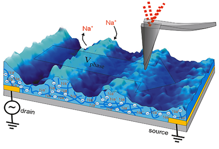
Figure: Schematic illustration of electrochemical strain waves (ESWs) generated in the channel of an electrochemical transistor. ESWs propagate into the device channel through combined charge transport and swelling.
References:
[1] F. Bonafè, J. Ji, S. Fabiano, B. Fraboni, T. Cramer, Small 2025, 10345, 1.
[2] F. Bonafè, M. Bazzani, B. Fraboni, T. Cramer, Nat. Commun. 2025, 16, 2499.
[3] S. Daboss, T. Cramer, N. Franke, B. Fraboni, C. Kranz, J. Microsc. 2025, 1.

Keynote Talk: 2D MoS2-based hybrid materials: structural, electronic and catalytic properties revealed by scanning probe microscopy
2D MoS2-based hybrid materials: structural, electronic and catalytic properties revealed by scanning probe microscopy
The absence of surface dangling bonds in two-dimensional crystals makes the controlled attachment of nanostructures, molecules or atoms particularly challenging. Conventional functionalization strategies often rely on extensive defect creation or harsh chemical treatments to provide anchoring sites; however, these approaches compromise the structural and electronic integrity of the host crystal. In this talk, I will present our recent efforts to develop synthesis strategies that enable the stable functionalization of 2D MoS₂ crystals while preserving their intrinsic properties. These approaches either exploit pre-existing defect sites or allow defect-free attachment of nanostructures and molecules on the MoS₂ surface. The resulting hybrid systems exhibit new structural and electronic features, giving rise to novel properties with potential relevance for catalysis and electronic applications. We employ a combination of scanning probe microscopy techniques, including atomic force microscopy (AFM) and scanning tunneling microscopy (STM), to characterize the atomic and electronic structure of these materials. In addition, scanning electrochemical cell microscopy (SECCM) is employed to map their catalytic activity with spatial resolution down to approximately 100 nm. Together, these techniques can provide a detailed nanoscale picture of how surface functionalization, local structure and electronic properties govern the catalytic behavior of MoS₂-based hybrid materials.

Keynote Talk: Electrochemistry in a Cage: How Steps, Defects and Molecular Confinement Drives the Solid–Liquid Interface Reactions
Electrochemistry in a Cage: How Steps, Defects and Molecular Confinement Drives the Solid–Liquid Interface Reactions
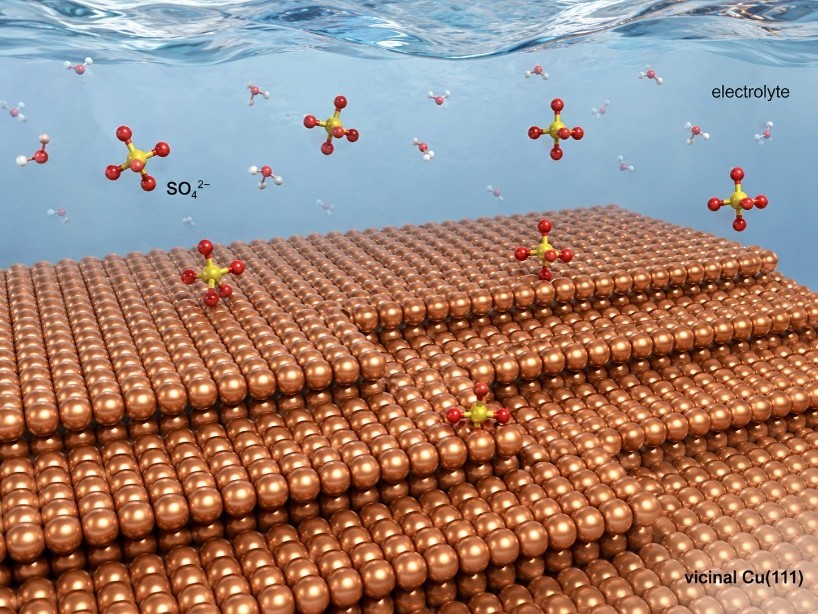
Electrochemistry is usually described through macroscopic observables: current, potential, charge transfer and reaction rates. Yet the elementary events that decide whether an electrode remains stable, reconstructs, corrodes, intercalates ions or activates catalytic pathways often take place in a far less ideal world: atomic steps, defects, nanocavities, molecular cages and buried interfacial regions. In this talk, I will argue that nanoscale physical confinement is not a geometrical detail of the electrode surface, but an active variable of electrochemical processes .
Starting from in situ and operando scanning probe microscopy studies at electrified solid–liquid interfaces, I will discuss how EC-AFM, EC-STM and complementary spectroscopies can reveal local transformations that are invisible to spatially averaged electrochemical measurements. Highly oriented pyrolytic graphite will be presented as a model system where anion intercalation, gas evolution, blister formation and subsurface oxidation challenge the classical picture of uniform and reversible graphite intercalation. The same conceptual framework will then be extended to vicinal metal surfaces and molecularly modified electrodes, where steps and terraces can be used to separate chemical driving forces from physical confinement effects.
The broader message is that the next generation of interface science should move beyond simply “imaging electrochemistry” toward engineering the local boundary conditions under which electrochemistry occurs . By combining nanomicroscopy, spectroscopy and controlled interfacial architecture, solid–liquid interfaces can become laboratories where reactivity, degradation and protection are not only observed, but spatially programmed.

Contributed Talk: Complementary C-AFM/XPS characterisation platform for battery-related materials
Complementary C-AFM/XPS characterisation platform for battery-related materials
M. Hývl 1, E.Tchernycheva 2, R.Dominko 2, M.Ledinský 1
1 Institute of Physics, Academy of Sciences of the Czech Republic, Cukrovarnická 10, 162 00 Prague 6, Czech Republic
2 Kemijski Inštitut, Hajdrihova 19, p.p. 660. SI-1001 Ljubljana, Slovenija
Abstract:
Li-ion batteries (LIBs) and other Li-based battery types (all-solid-state LiS-batteries – LS-SSB) are central to the ongoing energy transition, serving as critical energy storage solutions across various applications. For their further development, however, the electrode-electrolyte interfaces (EEI) and interphases and their crucial role in battery performance must be further studies and understood. The interphase's development is influenced by charge transfer reactions occurring at the EEI, which can trigger various degradation processes. While there is considerable understanding of anode-electrolyte interphases (SEI), the mechanisms behind cathode-electrolyte interphases (CEI) are less explored. This knowledge gap is partly due to the lack of effective techniques for characterizing CEI properties at different scales and conditions. The stability of cathode active materials at the EEI in the selected electrolyte directly correlates with battery cell performance and its cycle life. With most current applications relying on liquid electrolytes and emerging alternatives featuring solid polymer electrolytes, achieving a more comprehensive understanding of the CEI formation processes at micro- and nanoscales is crucial for making progress towards more stable battery performance.
X-ray photoelectron spectroscopy (XPS), has been heavily utilized to study both SEI and CEI due to its ability to detect both chemical composition and chemical oxidation states of the elements present at the very surface and up to the thickness of ~10 nm, with the spatial resolution from ~1 mm to ~10 microns. At its highest resolution, it can overlap with Atomic Force Microscopy (AFM). AFM techniques, such as C-AFM and C-AFM Topography, have enabled substantial advances in understanding the tight relationship between surface topography, electric current and mechanical properties.
In my presented research, I will demonstrate the results and lessons learned from the process of establishing the complementary C-AFM/XPS characterization platform. AFM measurements taken in the protective Argon atmosphere can be correlated with XPS measurements in order to access additional information not available by other characterization techniques, providing much-needed tool for multi-scale in-depth analysis of the EEI.

Contributed Talk: Beer–Lambert Law at the Nanoscale via Quantitative Infrared Nanospectroscopy
Beer–Lambert Law at the Nanoscale via Quantitative Infrared Nanospectroscopy
Masbah Ul Hakim,1 Francesco Simone Ruggeri,1
1Physical Chemistry and Soft Matter, Wageningen University & Research – Wageningen, The Netherlands (masbah.hakim@wur.nl, simone.ruggeri@wur.nl)
Abstract:
Quantifying molecular properties of materials at the nanoscale is essential for understanding functional interfaces, where small variations in film thickness, molecular organization and surface coverage can strongly influence material properties. Infrared spectroscopy is widely used for chemical analysis, identifying chemical groups through their characteristic vibrations. At the macroscopic scale, the Beer–Lambert law extends this capability to quantification by relating absorbance to the amount of absorbing material [1]. At the nanoscale, however, this scaling remains untested, because conventional infrared spectroscopy lacks the spatial resolution and sensitivity to probe molecular islands only a few nanometres thick. This leaves a fundamental open question: does Beer–Lambert scaling hold for molecular films of nanometre thickness? Answering this question is essential, because it determines whether nanoscale infrared spectroscopy can move beyond chemical identification toward quantitative measurement of local molecular content.
Here, we test whether Beer–Lambert law persists at the molecular scale by quantifying the infrared response of supramolecular films of well-defined nanometre heights. As a model system, we use self-assembled C16-benzene-1,3,5-triscarboxamide (C16-BTA) molecular films, which form laterally homogeneous crystalline islands with discrete molecular heights [2], as independently determined by atomic force microscopy. Using infrared absorption nanospectroscopy (AFM-IR), which combines molecular specificity with nanometre spatial resolution down to single-molecule sensitivity [3,4], we probe C16-BTA assemblies of different molecular heights. The integrated AFM-IR response exhibits a linear dependence on molecular film height across the investigated nanometre range, supporting Beer–Lambert law at the nanoscale. We further demonstrate how this height-calibrated response can be used to estimate effective surface concentrations within individual nanoscale domains.
These findings demonstrate that AFM-IR can move beyond chemical identification toward quantitative nanoscale spectroscopy of molecular thin films. This work provides a route toward quantitative chemical analysis of functional molecular interfaces at length scales inaccessible to conventional infrared spectroscopy.
References
[1]T. G. Mayerhöfer, S. Pahlow, and J. Popp, ChemPhysChem 21, 2029–2046 (2020).
[2]E. Weyandt, F. S. Ruggeri, E. W. Meijer, and G. Vantomme, J. Polym. Sci. 62, 2208–2214 (2024).
[3]F. S. Ruggeri, B. Mannini, R. Schmid, M. Vendruscolo, and T. P. J. Knowles, Nat. Commun. 11, 2945 (2020).
[4]X. Li, S. P. Pujari, J. van der Gucht, H. Zuilhof, and F. S. Ruggeri, Nat. Commun. 16, 6761 (2025).

Coffee Break
Contributed Talk: Noise diagnostics of memristive samples: full cycle noise measurements and AFM-based local fluctuation spectroscopy
Noise diagnostics of memristive samples: full cycle noise measurements and AFM-based local fluctuation spectroscopy
Resistive switching systems (aka memristors) are two-terminal electronic devices whose conductance state can be tuned in an analog fashion using voltage pulses above a threshold, while at subthreshold voltages the conductance state is preserved. In addition to the low power consumption, fast operation, and potentially sub-nanometer-scale active region of memristive devices, their analog programmability makes them particularly promising candidates for use as synaptic weights in hardware neural networks.
The inherent fluctuations in the active volume of memristive devices fundamentally determine their operation characteristics, for instance the device noise imposes severe constraints on the weight resolution in hardware neural network applications [1,2]. However, some probabilistic computing approaches require intentionally enhanced, and tunable noise levels [3,4]. Furthermore, the understanding of the noise properties also aids the understanding of the fluctuation sources and the optimizations of device fabrication [5].
Here, we present a comprehensive noise measurement methodology, which goes beyond the measurement of steady-state readout noise levels and tracks the voltage-dependent noise characteristics all along the resistive switching I(V) curves. This approach allows the detection of enhanced noise levels due to voltage-induced fluctuations, which may act as a precursor of the switching process [2]. We also discuss the implementation of this methodology as a local probe method, i.e. the possibility of noise measurement with a conductive AFM tip.
[1] Rao, M., Tang, H., Wu, J., Song, W., Zhang, M., Yin, W., ... & Yang, J. J. (2023). Thousands of conductance levels in memristors integrated on CMOS. Nature, 615(7954), 823–829.
[2] Nyáry, A., Balogh, Z., Sánta, B., Lázár, G., Jimenez Olalla, N., Leuthold, J., ... & Halbritter, A. (2025). Benchmarking stochasticity behind reproducibility: Denoising strategies in Ta₂O₅ memristors. ACS Applied Materials & Interfaces, 17(17), 25654–25662.
[3] Cai, F., Kumar, S., Van Vaerenbergh, T., Sheng, X., Liu, R., Li, C., ... & Strachan, J. P. (2020). Power-efficient combinatorial optimization using intrinsic noise in memristor Hopfield neural networks. Nature Electronics, 3(7), 409–418.
[4] Fehérvári, J. G., Balogh, Z., Török, T. N., & Halbritter, A. (2024). Noise tailoring, noise annealing, and external perturbation injection strategies in memristive Hopfield neural networks. APL Machine Learning, 2(1), 016107.
[5] Balogh, Z., Mezei, G., Pósa, L., Sánta, B., Magyarkuti, A., & Halbritter, A. (2021). 1/f noise spectroscopy and noise tailoring of nanoelectronic devices. Nano Futures, 5(4), 042002.

Contributed Talk: Chemical Analysis via Scanning Probe Microscopy by Park Systems
Chemical Analysis via Scanning Probe Microscopy by Park Systems
1A. Klasen,1Abdul Rauf
1Park Systems Europe GmbH, Schildkroetstraße 15, 68199 Mannheim, Germany
Modern applications have pushed materials research to the nanoscale, encompassing novel detector materials, energy storage systems, photocatalysts, and interfaces in general. Researchers need to understand and characterize a wide range of properties beyond mere topography, including electronic, mechanical, chemical, and electrochemical characteristics. However, the limited spatial resolution of conventional chemical and electrochemical characterization techniques has long posed a significant bottleneck. For example, infrared (IR) spectroscopy and ultramicroelectrodes for local electrochemical analysis are typically limited to the micrometer (µm) regime.
In this talk, we present Scanning Probe Microscopy (SPM) as a powerful platform for local chemical characterization. For example, by illuminating both the cantilever and the sample with a focused laser, local changes in the tip–sample interaction force enable infrared absorption to be measured with nanometer-scale spatial resolution and correlated with conventional SPM observables such as topography and mechanical properties.
Furthermore, we demonstrate how local electrochemical properties can be investigated using either cantilever-based approaches, such as Electrochemical Atomic Force Microscopy (EC-AFM) and Scanning Electrochemical Microscopy (SECM), or nanopipette-based techniques, including Scanning Electrochemical Cell Microscopy (SECCM) and the combined Scanning Ion Conductance Microscopy–Scanning Electrochemical Microscopy (SICM-SECM).
Overall, we showcase how Park Systems' Scanning Probe Microscopy provides a comprehensive toolkit for correlating chemical, electrochemical, mechanical, and topographical information with nanometer-scale spatial resolution.

Intro Session 4: Nanoscale Interface Metrology for Energy, Electronics and Molecular Materials
Keynote Talk: Seeing Phase-Change Materials Locally: Imaging Ellipsometry from Anisotropy to Reversible Optical Switching
Seeing Phase-Change Materials Locally: Imaging Ellipsometry from Anisotropy to Reversible Optical Switching
Low-loss phase-change chalcogenides such as Sb₂S₃ and Sb₂Se₃ are emerging as key materials for reconfigurable photonics because they combine large refractive-index tunability with negligible absorption across the visible and near-infrared. Yet their performance is not determined only by the average dielectric function. At the device scale, polycrystallinity, grain orientation, and local optical anisotropy can strongly affect phase accumulation, switching thresholds, and reproducibility.
In this keynote, I will discuss how imaging spectroscopic ellipsometry, imaging Mueller matrix polarimetry, and spatially resolved optical modeling can uncover the local dielectric response of these materials beyond conventional area-averaged measurements. Using Sb₂Se₃ thin films as a first example, I will show how differently oriented crystalline domains produce strong birefringence and dichroism and yield measurable refractive-index variations at telecommunication wavelengths. I will then extend this picture to Sb₂S₃, where anisotropy and polycrystalllinity have direct consequences for reversible laser-induced phase switching, including variations in amorphization thresholds and access to partial recrystallization states.
Together, these results show that controlling crystallographic texture is as important as minimizing optical loss. Imaging ellipsometry therefore offers a powerful bridge between local structure, dielectric function, and functional performance in next-generation programmable photonic devices

Keynote Talk: Spectroscopic ellipsometry as a characterisation technique for vdW materials
Spectroscopic ellipsometry as a characterisation technique for vdW materials
One of the earliest applications of ellipsometry was to measure the thickness of thin dielectric layers on a bulk substrate, most notably silicon dioxide on silicon. Later, spectroscopic ellipsometry provided important insights into the dielectric functions of semiconductors including gallium arsenide and silicon. Research on van der Waals (vdW) materials involves the study of materials that are sometimes are only one atom or unit cell thick. Initially such samples were exclusively produced by the exfoliation of flakes from bulk crystals. Such flakes, e.g. molybdenum disulfide, can be smaller than 50 microns x 50 microns in area, making imaging spectroscopic ellipsometry a powerful method of measuring the optical properties of the flakes. In recent years researchers have been directly growing vdW materials onto substrates using semiconductor epitaxial growth techniques. In Nottingham we are growing vdW materials using molecular beam epitaxy (MBE). For example, high temperature molecular beam epitaxy (HT-MBE) has been used to grow hexagonal boron nitride (hBN) on both highly oriented pyrolytic graphite (HOPG) and sapphire substrates [1]. The HT-MBE hBN can be grown with controlled amounts of dopants e.g. carbon [2]. By measuring the optical constants of exfoliated flakes of hBN using an Accurion EP4 imaging spectroscopic ellipsometer we can compare the properties of large areas ( ~ cm2) of hBN, grown by HT-MBE on sapphire, with those of flakes exfoliated from bulk grown material. We find that the exfoliated flakes have sharper band edge transitions than HT-MBE material and that ellipsometry can be used as a fast, non-destructive, characterisation technique to assist in the optimisation of growth parameters. iSE can also measure the local optical properties of HT-MBE grown hBN in the presence of inhomogeneities introduced onto the substrate. More recently MBE has been employed to grow gallium selenide (GaSe) on sapphire [3]. A potential application for GaSe is as a deep ultra-violet (DUV) photodetector. Spectroscopic ellipsometry can provide both the dielectric functions of the grown layer, which can be compared to theoretical predictions, and the extinction coefficients of the films in the DUV, helping to inform the photodetector design.
References:
1. T.S. Cheng, et al, J. Vac. Sci. Technol. B 36 (2) 02D103 (2018).
2. N. Mendelson, et al, Nature Materials 20 (3) 321 (2021).
3. M. Shiffa, et al, Small 20 (7) 2305865 (2024).

Lunch
Keynote Talk: Spectroscopic imaging ellipsometry for spatially resolved mapping of layer-by-layer oxidation in WSe2
Spectroscopic imaging ellipsometry for spatially resolved mapping of layer-by-layer oxidation in WSe2
F. Abualnaja1,2, G. Chu1, X. Lin1, H.-Y. Chen3, J.-J. Lin3, H. J. Joyce1, S. Hofmann1, L. W. Smith3, J.A. Alexander-Webber1,4
1Department of Engineering, University of Cambridge, 9 JJ Thomson Avenue, Cambridge CB3 0FA, UK
2Department of Electrical Engineering, King Fahd University of Petroleum and Minerals, Dhahran, Saudi Arabia
3Department of Physics, National Cheng Kung University, Tainan 701, Taiwan
4Department of Materials, Loughborough University, Loughborough, UK
Tungsten diselenide is a prominent candidate for nanoscale electronics and complementary metal–oxide–semiconductor technology due to its controllable p-type and n-type doping that is achievable through selective oxidation. However, characterizing the resulting oxide quality often relies on destructive or slow metrology. In this work, we demonstrate spectroscopic imaging ellipsometry (SIE) as a noninvasive technique to characterize the oxidation state of two-dimensional materials, providing spatially resolved measurements of layer thickness and uniformity [1,2,3]. We apply this method to compare few-layer WSe2 after thermal or plasma-based oxidation treatments. We show that plasma oxidation enables a highly controllable conversion of individual WSe2 layers into uniform sub-stoichiometric tungsten oxide (WOx), whereas thermal oxidation in atmospheric conditions yields a rough interface characterized by non-uniform oxide formation and blistering. Using SIE, we quantify a layer-by-layer conversion ratio, where a single WSe2 monolayer transforms into ∼1.6 nm of WOx during plasma oxidation. These findings, corroborated by atomic force microscopy, highlight the capability of SIE to resolve dielectric evolution and interface quality in layered semiconductors.
[1] Abualnaja et al. Applied Physics Letters, https://doi.org/10.1063/5.0320605 (2026)
[2] Potočnik et al. Nano Letters, Nano Letters 23, 5506 (2023)
[3] Potočnik et al. Small Methods 10, 2500437 (2025)
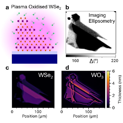
Figure 1: (a) Schematic crystal structure of multilayer WSe2. (b) Map of Δ across a 1-, 2-, 3-, and 4- layer oxidised WSe2 flake. Point by point fitted thickness of (c) WSe2 and (d) WO3 after oxidation.

Contributed Talk: Spatial dispersion in optical properties of square lattices of plasmonic particles revealed by Müller matrix ellipsometry
Spatial dispersion in optical properties of square lattices of plasmonic particles revealed by Müller matrix ellipsometry
E. Bortchagovskya,c, F. Daib, M. Fleischerb, D.R.T. Zahnc,d
a V.E.Lashkaryov Institute of Semiconductor Physics of NAS of Ukraine, Kyiv, 03028, Ukraine
b Institute for Applied Physics and Center LISA+, Eberhard Karls Universität Tübingen, D 72076 Tübingen, Germany
c Semiconductor Physics, Chemnitz University of Technology, D-09107 Chemnitz, Germany
d Center for Materials, Architectures, and Integration of Nanomembranes (MAIN), Chemnitz University of Technology, D-09107 Chemnitz, Germany
We demonstrate both experimentally and theoretically that spatial dispersion plays important role in the determination of optical properties of layers of plasmonic (interacting) nanoparticles. It results in the dependence of effective optical properties of such structures on the angle of incidence of the exciting light what is usually not considered in common treatment of data measured at different incidence. Additionally, we demonstrate that optical response of ordered lattices is the function of the mutual orientation of the lattice in relation to the plane of incidence despite formally such lattices are isotropic. Both effects can not be described by any standard dielectric tensor and demands the inclusion of the spatial dispersion.
Illumination of square lattice of circular symmetrical particles along any of four planes of symmetry (along rows or diagonal) produces no cross-polarization independently on the used wavelength keeping effective birefringence at inclined incidence due to elliptical shape of Fresnel zones. Such a birefringence is fixed by the plane of incidence, so effective optical constants along two orthogonal axes replace each other at the rotation of the lattice by 90°. At other non-symmetrical orientations cross-polarization arises what is well seen in measured Müller matrix. Such a behavior is shown in the Figure with color coded value of m13 element of the Müller matrix for the lattice of disc-like particles with the diameter 260 nm and the period 350 nm versus the orientation angle of the lattice in relation to the plane of incidence and the used wavelength. Spectra of ellipsometric angles measured along rows (0°) and along columns (rotated by 90°) also shown in the Figure coincide completely and demonstrate total coincidence of the resonance positions with the non-zero values of cross-polarization but gap mode when all field is concentrated between particles and their image in the substrate and no cross-talk of particles exists. It is the additional argument supporting the creation of the effective birefringence and spatial dispersion as the collective effect of interacting particles.
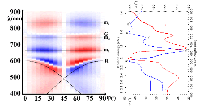
Color coded value of m13 element of the Müller matrix for the square lattice with the period 350 nm of gold discs with the diameter 260 nm versus the orientational angle and ellipsometric spectra measured at the orientation along the side of squares. Dotted line is the spectrum of the clean substrate.

Contributed Talk: Electrochemical variable angle spectroscopic ellipsometry of conducting polymer films at varied electrochemical doping
Electrochemical variable angle spectroscopic ellipsometry of conducting polymer films at varied electrochemical doping
Duško Čakara
Centre for Micro- and Nanosciences and Technologies(NANORI)
University of Rijeka, Croatia
dcakara@uniri.hr
Conducting polymers (CP) films are the main workhorse of organic electronics, rapidly bringing new materials to the technological fields of bioelectronic devices and organic solar cells. The conductivity of CP originates from delocalized charge carriers (in most cases holes) in the phonon-coupled electronic band structure, where the concentration of mobile electrons or holes is regulated by the oxidation (or “doping”) state of these molecules [1]. The optoelectronic properties of CP films, such as their refractive index dispersion, absorption spectrum and electronic conductivity may be derived from the (complex) dielectric function, fitted from the experimental ellipsometric spectra. The presentation brings forward such an experimental assessment for two archetypal CP film (PEDOT:PSS and p(g2T-T)) electrodes in contact with an aqueous ionic solution, under varied equilibrium electrochemical potential [2]. The fitting of the ellipsometric spectra and the deconvolution of the dielectric function was achieved by applying a Drude and several Lorentz terms, enabling the decomposition of the optical absorption in terms of electrons in the bound states, from those responsible for the hole-type conductivity. A possibility for modelling such experimental data is discussed in terms of a simple Nernstian redox isotherm.
[1] Kim E.-G., Bredas J.-L., Electronic Evolution of Poly(3,4-ethylenedioxythiophene) (PEDOT): From the Isolated Chain to the Pristine and Heavily Doped Crystals (2008) Journal of the American Chemical Society, 130, 16880–16889.
[2] Pathak G., Krasińska-Krawet Z., Szyk-Warszyńska L., Čakara, D., Doping of poly(3,4-ethylenedioxythiophene):poly(styrenesulfonate) films studied by means of electrochemical variable angle spectroscopic ellipsometry (2018) Thin Solid Films, 651, 31-38.

Contributed Talk: Imaging Spectroscopic Ellipsometry of 2D Materials: Dielectric Tensors and Unsupervised Clustering
Imaging Spectroscopic Ellipsometry of 2D Materials: Dielectric Tensors and Unsupervised Clustering
Sebastian Schaper1
1Park Systems GmbH, Göttingen, Germany
Imaging spectroscopic ellipsometry (ISE) merges the thin-film sensitivity of ellipsometry with microscope-level lateral resolution, allowing thickness and complex refractive index (n, k) to be determined non-destructively even for atomically thin multilayer systems. By measuring the change in polarization state upon reflection, ISE provides precise access to optical constants that are otherwise challenging to obtain, particularly for small-area 2D materials and heterostructures. In this way, ISE complements scanning probe techniques such as AFM: while AFM delivers true topography, ISE simultaneously yields optical thickness and dielectric information over large fields of view, without tip–sample interaction and overcomes the traditional sample-size limitation of ellipsometry down to individual exfoliated flakes. Operated in Mueller-matrix mode, ISE further extends to optically anisotropic samples, where combining measurements at several angles of incidence and sample azimuths enables the determination of the full dielectric tensor of individual crystalline domains [1], as will be demonstrated for a biaxial van der Waals material.
Each ISE measurement produces a rich hyperspectral dataset in which every pixel carries full spectra of ellipsometric data. To exploit this wealth of information efficiently, we employ unsupervised clustering: treating the wavelength-dependent response Ψ(λ), Δ(λ) of each pixel as a spectral fingerprint, clustering groups regions of similar optical response without manual segmentation or material-specific preprocessing. This provides an unbiased, natural reduction of the data dimensionality while preserving the optically meaningful contrast, and automatically identifies flakes, terraces, locally different layer thicknesses, residues, and substrate contributions. We demonstrate the workflow with hexagonal boron nitride (hBN), where representative cluster spectra serve as direct input for model-based extraction of layer thickness and optical constants. Since the approach relies on generic spectral features only, it transfers readily across the zoo of 2D materials, from semiconducting to insulating and metallic van der Waals crystals.
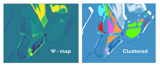
Figure 1: representative Ψ-map at 550 nm of hBN flake (left) and the clustered regions to be used for further ellipsometric analysis to determine optical constants and thickness of hBN flake regions (right)
[1] Grudinin, D. V., G. A. Ermolaev, D. G. Baranov, u. a. „Hexagonal Boron Nitride Nanophotonics: A Record-Breaking Material for the Ultraviolet and Visible Spectral Ranges“. Materials Horizons 10, Nr. 7 (2023): 2427–35. https://doi.org/10.1039/D3MH00215B.

Sponsor talks & Wrap up day 2 & Group Photo
Coffee Break
Hands-On Sessions
Break
Social Event
Welcome & Intro Session 5: Frontiers in AFM, SPM and Nanoscale Metrology
Keynote Talk: Strain-Tuned Phonon-Polaritons at LaAlO3 Twin Walls – An AFM, SNOM, Raman, and X-ray Study
NSFE-2026, 9-11 Sept 2026
Strain-Tuned Phonon-Polaritons at LaAlO3 Twin Walls –
An AFM, SNOM, Raman, and X-ray Study
Lukas M. Eng1,2,*, J. Wetzel1,2, J. Taboada-Gutiérrez3, M. Roeper1, F.G. Kaps1, G. Esposito3, D. Marchese3, R. Buschbeck1, P. Lenz1, J.M. Klopf4, H.A. Bechtel5, S.N. Gilbert Corder5,
J. Teyssier3, S.C. Kehr1, A.B. Kuzmenko3, and S.D. Seddon1,2
1. Institute of Applied Physics, Dresden University of Technology, Nöthnitzer Straße 61, 01187 Dresden, Germany
2. Würzburg-Dresden Cluster of Excellence (EXC2147) ctd.qmat – Complexity, Topology, and Dynamics in Quantum Matter, Dresden, Germany
3. University of Geneva, Department of Quantum Matter Physics (DQMP), Geneva 1211, Switzerland
4. Institute of Radiation Physics, Helmholtz-Zentrum Dresden Rossendorf, 01328 Dresden, Germany
5. Advanced Light Source (ALS), Lawrence Berkeley National Laboratory, Berkeley, CA 94720, USA
* Corresponding author: lukas.eng@tu-dresden.de
Investigating dynamically strain-tuned material properties in-situ by AFM techniques is of uttermost interests, since shedding light on how macroscopic stimuli directly impact at the atomic and nanometer length scale, i.e. altering the electronic, magnetic, dielectric, optical, and topological information. Here, we combine strain-tuning with AFM topography and scanning-near-field optical microscopy (SNOM) investigations, to steer and switch THz phonon-polaritons (PhPs) that run along LaAlO3 twin walls (see Fig. 1).
Funneling and directing THz light has witnessed great attention for the last decade, and are said to foster a clue technology for lossless on-chip communication at ultrahigh speeds. Success was documented through THz light confinement orders of magnitudes below the free-space diffraction limit [1], as well as by light canalization, for instance in twisted van-der-Waals materials [2].
Here we focus on a completely new class of materials, so-called ferroelastics, that bear as their characteristic, naturally occurring twin walls (TWs), i.e. crystallographically pure, stress-free 2D-sheets that separate two domains of opposite optical axis and structural orientation through mirror planes. We experimentally demonstrate here that electromagnetic fields running along these twin walls, are confined to better than 260-times the free-space wavelength, and further corroborate these findings theoretically with both COMSOL modeling and the extended analytical dipole model [1]. Moreover, these canalized PhPs can be easily (de)tuned from resonance to non-resonance through both (i) accurate THz laser wavelength adjustment within < 0.1 THz, and (ii) mechanical straining [3]. In fact, applying an uniaxial compressive strain to the LaAlO3 single crystal induces a 2nd order structural phase transition from rhombohedral to orthorhombic at room temperature, hence reproducibly switching these PhPs on-and-off. Our nanoscale, AFM-based findings are well backed up with mesoscopic experimental investi-gations, using one and the same sample mounted also for µ-Raman and X-ray analysis under strain.
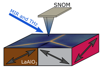
Fig. 1: Scanning near-field optical microscopy (SNOM) at LaAlO3 twin walls (TWs). An AFM-tip is illuminated with MIR to THz light, allowing for probing the optical phonon-polariton confinement at LaAlO3 TWs.
References
[1] J. Wetzel et al., Nature Commun. (2026) submitted; https://arxiv.org/abs/2603.22013
[2] M. Obst et al., ACS Nano 17, 19313 (2023); https://doi.org/10.1021/acsnano.3c06477
[3] E. Singh et al., Phys. Rev. B 106, 144103 (2022); https://doi.org/10.1103/PhysRevB.106.144103

Keynote Talk: Interphases in Modern Battery Materials
Interphases in Modern Battery Materials
LiNi 0.5 Mn 1.5 O 4 (LNMO) is a promising cathode material owing to its high operating potential of 4.75 V vs Li⁺/Li. However, the high potential triggers electrolyte oxidation. A mechanically robust cathode–electrolyte interphase (CEI) is essential for maintaining structural integrity of high-voltage lithium-ion batteries. The CEI layer functions as a protective barrier that suppresses parasitic reactions under high-voltage conditions. CEI layers are thin (< 20 nm). Therefore assessing their elastic properties is challenging. We applied the scanning force microscopy method which enablinges quantitative mechanical characterization of thin CEI layers on rough composite electrodes surfaces. The pristine crystalline LNMO surface exhibited an elastic modulus of approximately 126±20 GPa, whereas the binder/carbon (b/c) regions had a modulus of 1.9±0.1 GPa. After 200 charge discharge cycles, the elastic modulus became homogeneous with the moduli on the LNMO and b/c regions reaching≈4 GPa.
This mechanical convergence is supported by a convergence in chemical composition of the interphase between the LNMO and b/c regions. This work provides understanding of interfacial stability and establishes a robust and reproducible framework for quantifying the elastic modulus of interphase layers within composite electrodes, providing insights for the design of stable high-voltage battery systems.
Reservoir-free batteries are designed without a traditional anode material in the manufacturing process. Instead, a current collector is used. When the battery is charged for the first time, lithium deposits onto this collector effectively forming the anode in place. We investigated interface and interphase of the solid electrolyte and current collector materials with operando Kelvin Probe Force Microscopy (KPFM) [2], [3].
These examples that illustrate Scanning Force Microscopy methods are versatile and beneficial for characterizing and understanding batteries and their components.
References:
[1] X. Shi, F. Weber, H.-J. Butt1, R. Berger, Mechanical Properties of Cathode Electrolyte Interphase Layers in High-Voltage Lithium-Ion Batteries, Journal of Materials Chemistry A 2026, doi:10.1039/d5ta09458e.
[2] F. Weber, Till Fuchs, S. Kobayashi, X. Shi, L. Shen, T. Hitosugi, J. Janek, R. Berger, submitted for publication 2026.
[3] F. Weber, C. Zhu, S. Kobayashi, T. Fuchs, T. Hitosugi, J. Janek, R. Berger, Interpretation of Kelvin Probe Force Measurements in Solid-State Electrochemical Cells. ACS Applied Materials & Interfaces 17 (42), pp. 58825 - 58836 (2025).

Keynote Talk: Quantitative advanced SPM data processing with Gwyddion
Quantitative advanced SPM data processing with Gwyddion
To make a SPM measurement quantitative, we need to focus on different aspects:
to choose suitable calibration samples, to operate the instrument the right way and to process the data obtained from the set of measurements appropriately. With advent of novel measurement regimes that extend SPM capabilities in measurement of complex mechanical, electrical, thermal magnetic or optical properties, the complexity of all the three tasks only grows.
This talk will focus on tools that can be used within Gwyddion open source software to make at least parts of it easier. This includes methods for reducing uncertainty of measurements by proper choice of scan area and resolution with respect of the measured surface topography, by choice of reference samples and by use of methods for processing and further using the data from reference samples in different SPM modalities.
Talk will also focus on processing advanced data obtained in novel measurement regimes, like individual force-distance curves coming from off-resonance tapping regimes, high-speed image stacks or volume data representing some field distribution above the sample surface, demonstrating Gwyddion capabilities in this direction and comparing the benefits and drawbacks of storing and post-processing the complex datasets instead of their real-time analysis.

Keynote Talk: Diving into the Atom – 40 years of AFM
Diving into the Atom – 40 years of AFM
Franz J. Giessibl
Experimental and Applied Physics, University of Regensburg, 93053 Regensburg, Germany
franz.giessibl@ur.de
When Binnig and Rohrer provided stunning images of the atoms of the silicon 7x7 reconstructed surface with the scanning tunneling microscope (STM) [1], it came as a surprise and many initially believed they were fake. STM relies on a quantum effect, electron tunneling, with its exponential increase at a factor of ten per Å (100 pm) between two biased conductive electrodes. The strong increase of current with distance reduction is key to the high spatial resolution of STM and its monotonicity facilitates distance feedback. In 1986, Binnig, Gerber and Quate introduced atomic force microscopy (AFM) [2], a method that also images samples by probing the atomic surface arrangement of a sample with, ideally, the single front atom of a sharp tip. Richard Feynman believed that the atomic hypothesis (“…attracting each other when they are a little distance apart, but repelling upon being squeezed into one another”) contains the most scientific information in the fewest words and started chapter 1 of his Feynman Lectures on Physics [3] with this statement. The AFM uses exactly these properties of atoms to create images – it senses a surface with a sharp tip mounted on a cantilever. The challenge is that this sensor needs to be able to probe forces small enough such that neither the tips front atom nor the sample are damaged on an atomic level. The silicon 7x7 surface was first resolved by AFM in a noncontact mode [4], where the frequency shift of an oscillating cantilever was used as a feedback mechanism [5]. Further progress was enabled by the invention of the qPlus sensor, a quartz cantilever that is self sensing and oscillates at sub-Angstrom amplitudes [6]. Outfitting its tip with a CO molecule allows to image organic molecules at unprecedented resolution [7]. To our knowledge, today AFM provides the greatest spatial resolution of all microscopes by resolving structures within single atoms [8,9]. The quantum corral, introduced by Crommie, Lutz and Eigler in 1993 [10], was revisited by AFM in 2021, showing that the 102 electrons that the corral contains can be viewed as the shell of a two-dimensional atom with similar bonding properties to AFM tips as a natural atom [11]. AFM is now a powerful tool for the surface science of insulators in ultrahigh vacuum [12]. By far the most applications of AFM are in ambient conditions. Therefore, we trust that Park Systems new microscope NX1, an ambient AFM that can also use the qPlus sensor based on our Orpheus II microscope [13] will enable many new discoveries.
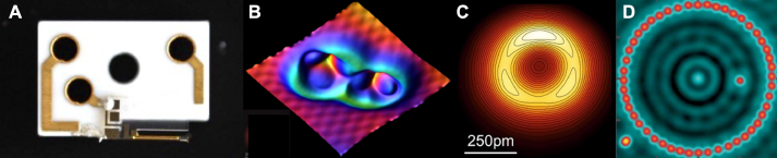
A qPlus sensor. B AFM image of a Fe trimer next to a Fe dimer on Cu(111). C AFM image of a single Fe atom on Cu(111)2,6. D Quantum corral with one perturbing atom.7
References
1. G. Binnig et al., Phys. Rev. Lett. 50 120 (1983).
2. G. Binnig et al., Phys. Rev. Lett. 56 930 (1986).
3. R. P. Feynman et al., The Feynman Lectures on Physics, Addison Wesley 1963.
4. F. J. Giessibl, Science 267, 68 (1995).
5. T. R. Albrecht et al., J. Appl. Phys. 69, 668 (1991).
6. F. J. Giessibl, Rev. Sci. Instrum. 90, 011101 (2019).
7. L. Gross et al., Science 325 1110 (2009).
8. M. Emmrich et al., Science 348 308 (2015).
9. F. Huber et al., Science 366 235 (2019).
10. M.F. Crommie, Science 2623 218 (1993).
11. F. Stilp et al., Science 372 1196 (2021).
12. J. Hütner et al., Science 385 1241 (2024).
13. K. Pürckhauser et al., Rev. Sci. Instrum. 91, 083701 (2020).

Coffee Break
Keynote Talk: Feeling the Lattice: AFM as a Real-Space Probe of Charge Transport in Organic Semiconductors
Feeling the Lattice: AFM as a Real-Space Probe of Charge Transport in Organic Semiconductors
Organic semiconductors are prized for their mechanical flexibility, which raises a basic question: does softness limit how well they transport charge? The link turns out to be more intimate than it first appears. Macroscopic stiffness is the long-wavelength, zero-frequency limit of the acoustic phonon response, and the low-energy phonons it reflects are precisely those implicated in charge transport. Mechanics and electronics are therefore not separate properties of these materials but two readings of the same underlying structure.
Atomic force microscopy is the natural tool for probing this link directly, because it captures both molecular order and nanomechanics in real space — on the same
surface, under ambient conditions — as a real-pace counterpart to the reciprocal-space picture from X-ray scattering. I will show how higher-eigenmode imaging resolves polymer packing below one nanometre [1], while force-distance based nanomechanical mapping charts local stiffness across the same regions. Across semicrystalline polymers, nanoscale stiffness tracks structural order [2] — and, more tellingly, stiffness tracks carrier mobility. In the polymer PBTTT, nanomechanical texture evolves across amorphous, terraced, and ribbon phases. In a series based on small-molecule crystals of alkylated DNTT, side chains that expand the unit cell soften the crystal out of plane yet stiffen it in plane, in step with mobility [3].
Taken together, these results point to a common structural origin for mechanics and electronics in molecular materials and establish nanomechanical AFM as a tactile complement to scattering — reading structure in real space, where it matters most for transport.
References
[1] I. Dobryden, V. V. Korolkov, … D. Venkateshvaran, Nature Communications 13, 3076 (2022)
[2] S. Cristofaro D. Brandt, … Y. Olivier et al., Journal of Materials Chemistry C 13, 15506 (2025)
[3] K.-H. Hwang, D. Brandt, … D. Venkateshvaran, Nature Communications 17, 1621 (2026)

Keynote Talk: Phase nanoengineering in condensed matter for nanoelectronic applications
Phase nanoengineering in condensed matter for nanoelectronic applications
Phase nanoengineering enables the nanoscale tailoring of the physical properties of condensed matter systems using highly localized heating with focused lasers or thermal probes. Here, we summarize this approach through three examples: the control of spin waves in magnetic oxides, the patterning of magnetization textures in metallic multilayers, and the tuning of superconductivity in cuprate thin films.
In magnetic oxides such as YIG, laser-induced phase modification produces confined three-dimensional changes in the magnetic properties, enabling the engineering of the spin-wave band structure, and the realization of complex integrated magnonic circuits.
In metallic multilayers we show the grayscale tuning of the magnetic properties, leading to the creation of hidden magnetic information storage patterns and “moiré magnetic textures”.
In YBCO, a prototypic high-temperature cuprate superconductor, direct laser writing locally modifies superconducting properties, including critical temperature and current density, through thermally driven oxygen redistribution.
In all these examples nanoscale characterization tools such as scanning probe microscopy and optical methods provide direct access to the magnetic, electronic, and transport properties of the engineered phases.
The direct manipulation of the physical properties of condensed matter, beyond conventional nanofabrication, opens up unforeseen possibilities for the design of new advanced materials and functionalities in nanoelectronics.

Keynote Talk: Characterizing functional paper and paper fibers with the atomic force microscope
Characterizing functional paper and paper fibers with the atomic force microscope
Robert Stark
Technische Universität Darmstadt, Institute of Materials Science, Peter-Grünberg-Str. 16, 64287 Darmstadt
Paper is one of the most widely used and sustainable materials in modern society. Produced primarily from renewable resources such as wood, it combines high recyclability with complete biodegradability. Owing to its unique fluidic, mechanical, and interfacial properties, paper is indispensable in applications including printing, packaging, and hygiene products. Beyond these conventional uses, it also offers considerable potential for advanced technologies, including lightweight materials for mobility, medical sensors, and 4D-printed soft robots ("paperbots"). Realizing these applications requires a deeper understanding of how functionalization, aging, recycling, and environmental conditions influence the mechanical properties of individual fibers, fiber joints, and small fiber networks. The atomic force microscope (AFM) is well suited to address these questions by linking fiber structure, chemistry, and mechanics at the nanoscale.
AFM provides complementary characterization methods: high-resolution imaging reveals the distribution of polymers and the effects of functionalization, while indentation experiments quantify local mechanical properties. Nanoindentation with sharp tips enables surface and near-surface characterization of cellulosic fibers at nanometer resolution, whereas colloidal probe measurements capture mechanical heterogeneities over larger length scales. These nanomechanical measurements provide key parameters for numerical models that predict the behavior of fibers and paper networks. Furthermore, AFM studies under controlled humidity offer valuable insights into moisture-dependent mechanics and the actuation mechanisms of paper-based actuators. Nevertheless, the hierarchical, heterogeneous, and highly compliant structure of cellulose fibers presents significant challenges for quantitative nanoscale characterization.
Closing Remarks, best Contributive Talk and Poster & Thank you
Lunch