Electrical AFM Characterization of Devices Using an Integrated Multi-Probe Platform
- 19 May 2026
- Volume 30
- NANOscientific Magazine, 2026
Jay Son¹, Edward Park¹, Luna Kim¹, John Park¹, Charles Kim¹, James Kerfoot², Andrea Cerreta²
¹Park Systems Corp., Gwacheon, South Korea ²Park Systems GmbH, Mannheim, Germany
Introduction
As research on next-generation semiconductor devices and two-dimensional (2D) materials continues to accelerate, there is growing demand for measurement platforms capable of probing both electrical behavior and nanoscale surface properties simultaneously. Atomic force microscopy (AFM) has long been an essential tool for nanoscale characterization, providing high-resolution imaging alongside electrical and mechanical measurements¹˒². However, advanced electrical AFM techniques—such as Kelvin probe force microscopy (KPFM), conductive AFM (C-AFM), and scanning thermal microscopy (SThM)—often require precise electrical contacts to nanoscale devices while scanning, creating significant experimental challenges³˒⁴.
In many laboratories, these contacts are made using external probe stations or manual probing approaches. While functional, such configurations frequently introduce complications including mechanical interference with the AFM scanner, poor reproducibility, limited placement precision, and additional mechanical loading on the sample stage. Large manipulators or external stages may also reduce stability during high-resolution AFM imaging.
To address these limitations, Park Systems and Imina Technologies have developed an integrated solution combining Park Systems AFM instrumentation with the Imina Technologies Microprobing Platform (4-Bot). In this configuration, up to four independently controlled miBot™ micro-robotic probes are mounted directly inside the AFM stage environment. Each miBot unit can be positioned with micrometer-scale precision to establish electrical contacts with the sample while maintaining full compatibility with AFM scanning.
The tungsten probes mounted on the miBot units can be connected directly to the auxiliary input/output channels of the AFM controller, enabling simultaneous source–drain biasing and electrical measurements during AFM operation. The integrated platform therefore enables multi-electrode device characterization and high-resolution nanoscale imaging within a single instrument.
This article outlines the integrated hardware configuration and demonstrates three representative applications enabled by this platform:
- Electrical contacting of layered materials and layered material heterostructures on insulating substrates
- In-operando nanoscale voltage mapping in lateral field-effect transistors
- Measurement of Joule heating in nano-structured electronic devices
Together, these examples illustrate how the integrated system enables advanced electrical and thermal AFM characterization with improved flexibility and experimental control.
Integrated Hardware Platform
The experimental setup was configured by integrating a Park Systems FX200 AFM with the Imina Technologies Microprobing Platform (4-Bot). The probe station is mounted directly onto the FX200 sample chuck, allowing electrical probes to be positioned precisely near the region of interest without interfering with the AFM cantilever.
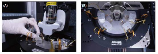
Each miBot unit is magnetically anchored to the AFM stage, allowing rapid manual installation or removal. Up to four units can be positioned simultaneously, providing independent multi-electrode contacts for device measurements. The probes are manipulated using a dedicated positioning controller and a PC-connected control pad, which allows precise control of probe movement speed and direction.
An example configuration is shown with a device containing patterned gold electrodes placed on the FX200 stage. The AFM cantilever is first positioned near the region of interest. Tungsten probes mounted on the miBot units are then carefully aligned with the device contact pads. The alignment process is facilitated by the high-resolution optical vision system of the AFM and the intuitive operation of the Precisio™ software.
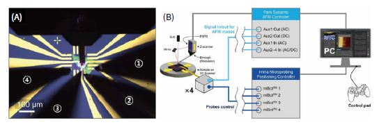
Electrical connections are made through the AFM controller’s auxiliary channels. In the configuration used in this study:
- Aux1 Out and Aux2 Out supply AC or DC drive signals to the device
- Aux1 In and Aux2–4 In acquire electrical response signals from the device
This configuration enables simultaneous electrical excitation and measurement while the AFM performs nanoscale imaging. Because each miBot probe can be positioned independently, the system supports flexible multi-probe measurement configurations, including two-probe and four-probe device geometries.
The integrated system therefore provides a unified platform for studying nanoscale electrical behavior while maintaining stable AFM operation.
Electrical AFM of Electrically Floating Layered Materials
Layered materials (LMs) and layered material heterostructures (LMHs) have become key platforms for next-generation nanoelectronic devices. AFM-based electrical techniques such as conductive AFM and Kelvin probe force microscopy are widely used to study these materials, enabling nanoscale measurements of conductivity, potential distribution, and interfacial phenomena⁵.
However, these techniques generally require reliable electrical contacts. Conventional approaches often involve lithographic patterning and deposition of metal electrodes, which can complicate sample preparation and make it difficult to study materials during intermediate fabrication stages⁶.
Using the miBot microprobing system, electrical contacts can instead be applied directly to individual flakes of layered materials placed on insulating substrates.
In one experiment, a tungsten probe was positioned to contact a graphite region connected to a few-layer graphene (FLG) flake. The miBot contact served as a grounding point, preventing charge accumulation during KPFM measurements while simultaneously acting as a drain electrode during conductive AFM imaging.
To demonstrate the effect of grounding, local anodic oxidation was used to create channels that divided the FLG flake into electrically isolated regions. These channels completely separated portions of the flake from the contacted region.
AFM measurements revealed that the isolated regions developed distinct electrical potentials due to charge accumulation. In contrast, the region connected to the miBot probe remained electrically stable. Current mapping performed with C-AFM confirmed that current flow occurred only within the electrically contacted portion of the flake.
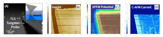
This experiment demonstrates that direct electrical contacting using miBot probes enables stable electrical AFM measurements on layered materials without the need for pre-fabricated electrodes.
Electrical Characterization of Layered Material Heterostructures
The ability to electrically contact individual flakes also enables advanced characterization of layered material heterostructures.
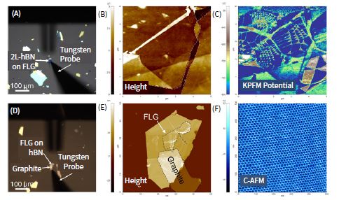
One example involved heterodyne Kelvin probe force microscopy (HD-KPFM) measurements of a ferroelectric superlattice formed between two parallel stacked hexagonal boron nitride (hBN) layers on a few-layer graphene substrate deposited on SiO₂.
Single-pass HD-KPFM imaging revealed nanoscale variations in surface potential associated with the ferroelectric superlattice structure. The electrical grounding provided by the miBot probe was essential for stable measurements, since the KPFM tip bias would otherwise charge the flake and cause drift in the measured potential.
A second demonstration involved contacting a graphene flake aligned with a ~25 nm thick hBN layer on a mica membrane supported by PDMS. In this case the layered structure was still on the fabrication stamp used during heterostructure assembly.
Non-contact AFM imaging combined with conductive AFM revealed a moiré pattern between the graphene and hBN layers. The ability to perform electrical characterization directly on the fabrication stamp enables researchers to verify layer alignment and interfacial properties before additional fabrication steps are performed.
This capability reduces the risk of continuing nanofabrication on misaligned structures and allows researchers to study interfaces that may later become buried during device processing.
In-Operando KPFM of MoS₂ Field-Effect Devices
The integrated multi-probe platform also enables in-operando AFM measurements of operating electronic devices.
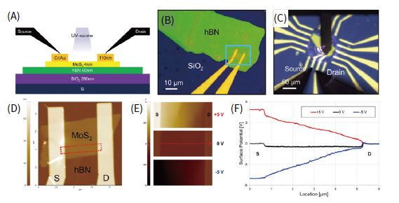
In this study, a MoS₂ thin-film device was fabricated by transferring a ~4 nm exfoliated MoS₂ flake onto a ~60 nm hBN layer deposited on a Si substrate with 280 nm thermal SiO₂. Source and drain electrodes composed of Cr/Au (10 nm/100 nm) were patterned using electron-beam lithography.
Local UV-ozone treatment was applied to selected regions of the MoS₂ channel to induce partial oxidation and modify the electronic properties of the device⁷⁻⁹.
For AFM measurements, two tungsten probes mounted on miBot units were placed on the source and drain electrodes. The AFM cantilever was positioned above the MoS₂ channel to perform Kelvin probe force microscopy.
During the experiment:
- The drain electrode was held at 0 V (ground)
- The source electrode was sequentially biased at −5 V, 0 V, and +5 V
KPFM surface potential maps were acquired for each bias condition.
The measurements revealed clear bias-dependent changes in the potential distribution across the channel. Line profiles extracted from the KPFM images showed that the potential at the source electrode accurately reflected the applied bias. A nearly linear potential drop was observed along the MoS₂ channel between the source and drain contacts.
This in-operando KPFM technique enables quantitative extraction of contact resistance and analysis of potential drop distributions within nanoscale devices. By comparing measurements obtained under different bias conditions, researchers can identify spatial variations in resistance, edge-related effects, and other localized transport phenomena.
Combining KPFM imaging with electrical measurements such as current–voltage (I–V) and gate-dependent transport measurements further enables correlations between the spatial potential landscape and the overall electronic behavior of the device.
Scanning Thermal Microscopy of Nano-Structured Devices
Beyond electrical characterization, the integrated platform also enables thermal measurements of nanoscale devices under electrical operation.
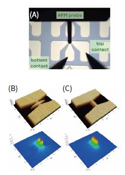
Scanning thermal microscopy (SThM) experiments were performed on nano-structured devices consisting of chains of nano-constrictions connected between large electrodes. These structures form spin Hall nano-oscillator chains¹⁰⁻¹².
Each device was electrically connected to top and bottom electrode pads, which were contacted using tungsten probes mounted on the miBot units. A Keithley Instruments 2636B source meter was used to inject constant DC current through the devices.
Thermal measurements were performed using the AppNano VertiSense™ SThM module with thermocouple-based AFM probes. The thermocouple voltage measured by the probe can be converted into temperature after calibration.
During the experiment, a constant 2 mA DC current was applied through the device while topography and thermal maps were acquired simultaneously.
The SThM measurements revealed localized temperature increases at the nano-constrictions. These locations correspond to regions where current density is highest, producing increased Joule heating.
By systematically varying the injected current, researchers can observe how thermal response evolves with electrical loading. Such measurements also allow identification of non-uniformities between constrictions that may indicate increased resistance or imperfect electrical connectivity.
This approach provides direct visualization of thermal hotspots and current crowding effects in nanoscale electronic devices.
Conclusions
The integration of the Park Systems FX200 AFM with the Imina Technologies Microprobing Platform (4-Bot) provides a powerful and flexible platform for advanced electrical and thermal characterization at the nanoscale.
By enabling precise alignment of miBot-mounted tungsten probes with the AFM cantilever inside the FX200 instrument, stable electrical contacts can be established while maintaining interference-free AFM scanning. This configuration allows simultaneous device biasing, electrical measurements, and high-resolution AFM imaging.
Several application examples demonstrate the capabilities of the integrated platform:
Electrical contacting of individual layered materials and layered material heterostructures on insulating substrates
In-operando Kelvin probe force microscopy mapping of voltage distribution in MoS₂ field-effect devices
Scanning thermal microscopy visualization of Joule heating in nano-structured electronic devices
For layered materials research, the ability to electrically contact individual flakes without lithographic processing provides significant experimental flexibility. For device characterization, the system enables direct visualization of potential distributions, contact resistance effects, and thermal hotspots during device operation.
These results demonstrate that the combination of Park Systems AFM technology and the Imina Technologies microprobing platform provides an integrated solution for nanoscale electrical and thermal characterization of 2D materials and thin-film electronic devices.
References
- Wang, Qing Hua, et al. "Electronics and optoelectronics of two-dimensional transition metal dichalcogenides." Nature nanotechnology 7.11 (2012): 699-712.
- Schwierz, Frank, Jörg Pezoldt, and Ralf Granzner. "Two-dimensional materials and their prospects in transistor electronics." Nanoscale 7.18 (2015): 8261-8283.
- Melitz, Wilhelm, et al. "Kelvin probe force microscopy and its application." Surface science reports 66.1 (2011): 1-27.
- Wagner, Tino, et al. "Kelvin probe force microscopy for local characterisation of active nanoelectronic devices." Beilstein journal of nanotechnology 6.1 (2015): 2193-2206.
- Sequeira, Ian, et al. "Manipulating moires by controlling heterostrain in van der Waals devices." Nano Letters 24.49 (2024): 15662-15667.
- Vizner Stern, Maayan, et al. "Interfacial ferroelectricity by van der Waals sliding." Science 372.6549 (2021): 1462-1466.
- Ma, Xiaolei, et al. "Defects induced charge trapping/detrapping and hysteresis phenomenon in MoS₂ field-effect transistors: mechanism revealed by anharmonic Marcus charge transfer theory." ACS Applied Materials & Interfaces 14.1 (2021): 2185-2193.
- Park, Youngseo, et al. "Thermally activated trap charges responsible for hysteresis in multilayer MoS₂ field-effect transistors." Applied Physics Letters 108.8 (2016).
- Shin, Beomkyu, et al. "Half-Oxidized MoS₂-Based Memristor by UV-Ozone Treatment." ACS Applied Electronic Materials 7.9 (2025): 3737-3743.
- Bodzenta, Jerzy, and Anna Kazmierczak-Bałata. "Scanning thermal microscopy and its applications for quantitative thermal measurements." Journal of Applied Physics 132.14 (2022).
- Tovee, Peter D., et al. "Nanoscale resolution scanning thermal microscopy using carbon nanotube tipped thermal probes." Physical Chemistry Chemical Physics 16.3 (2014): 1174-1181.
- Kumar, Akash, et al. "Robust mutual synchronization in long spin Hall nano-oscillator chains." Nano Letters 23.14 (2023): 6720-6726.
