Primer: Surface Analysis Techniques Using Atomic Force Microscopy
- 03 Nov 2023
- Volume 25
- NANOscientific Magazine, Fall-Winter 2023
Introduction
Atomic force microscopy (AFM) is a nano-scale microscopy technology that employs a sharp cantilever featuring a probe tip with a width less than 10 nm. By gauging the displacement of this cantilever, AFM detects atomic forces – both attraction and repulsion – occurring between the probe tip and the sample surface. A super luminescent diode (SLD) light source is utilized to monitor the cantilever's displacement (refer to Figure 1). The motions of the sample and cantilever in the X, Y, and Z directions are controlled by piezoelectric scanners. Through these mechanisms, precise three-dimensional topography data of the sample surface can be captured. This topography data forms the basis for various applications, with specific measurement modes chosen depending on the application's requirements.
The evolution of AFM is underpinned by the integration of three distinct application techniques, each contributing to high-resolution three-dimensional topography quantification. technique A involves surface scanning using a probe, enabling simultaneous measurement of mechanical, electrical, and chemical properties at the same locations on the sample. technique B, on the other hand, doesn't require scanning; it involves moving the Z axis of the scanner to make the probe "contact and separate" from the sample. The force/distance curve plotted from cantilever deflection and deformation during this process quantitatively determines the interaction force between the probe and the sample. Lastly, technique C employs the probe for tasks such as indentation, scratch tests, and wear tests on the sample surface. Additionally, it serves as a tool for mechanical processing, anodization-based surface patterning, and mechanical property assessment, distinct from the usage scenario of technique B.
and the SLD is used to detect the displacement
of the cantilever caused by the change in surface height.
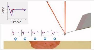
Technique A: Property Mapping
This is an example that shows the topography, surface potential, and magnetic force of a two-phase stainless steel with Austenite and Ferrite organizations that are coexisting [1]. The scan size is 20 μm x 20 μm, and the magnetic film was coated with a probe to measure the topography information, electrical information, and magnetic information simultaneously.
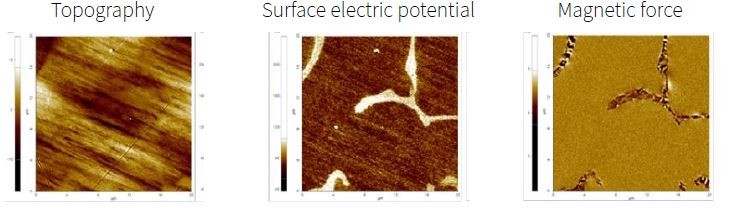
The topography information of the polished sample surface was flat, and it was difficult to identify the two materials from the topography, but it was possible to identify them from the electrical and magnetic properties (Figure 2). Regarding the phase separation of the solid solution in which Ferrite was mixed to reinforce the stress corrosion cracking, which is a disadvantage of the Austenite system, the Ferrite phase has a strong magnetism. This can be seen as a striped pattern when viewed with a Magnetic force microscope (MFM). The paramagnetic Austenite phase, however, is uniform. The Kelvin probe force microscope (KPFM) can measure the difference in work function between the two materials. This is done by measuring the contact potential difference between the conductive probe and the sample surface.
The KPFM image shows that the surface potential of the Ferrite phase is higher than that of the Austenite phase.

Obtain the force/distance curve at each data
point. Different parts of the material change the
topography of the force/distance curve.
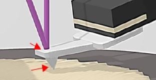
Technique B: Nanomechanical Characterization
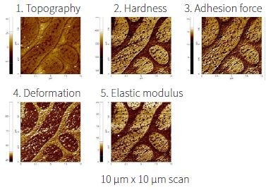
First, we introduce the evaluation of elasticity, adhesion, and deformation by PinPoint nanomechanical mode. When obtaining the force/distance curve, quantitative measurement of local elasticity, adhesion, and deformation can be performed if the spring constant of the cantilever is pre-calibrated. There is a method called PinPoint nanomechanical mode [2]. (Figure 3) to obtain the force/distance curve for each data point in the scan area, which is often used for evaluation of the dissolved membrane.
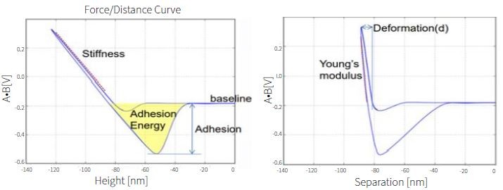
By considering the force/distance curve obtained and the amount of pressing to the sample of cantilever, the mechanical properties such as Young's modulus, deformation amount, adhesion force and hardness can be quantitatively calculated from the force/separation curve as shown in Figure 4. As an example of membrane measurement, the results obtained by PinPoint nanomechanical mode for polished surface PS-PVAc film, which is widely used for coating material and packaging material, are shown. Clear phase separation of polyvinyl acetate (PVAc) in the matrix part (sea) and polystyrene (PS) island is observed. It indicates that PS is harder than matrix PVAc, and it has a large adhesive force, a small amount of deformation, and a high elastic modulus.
properties at the same location as the topography
image on the upper left
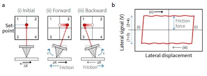
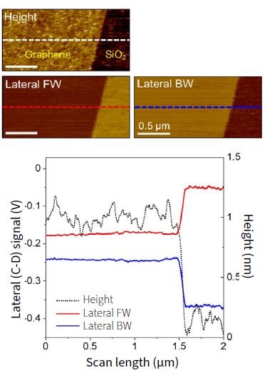
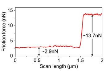
Moving on, we delve into the assessment of friction forces through the utilization of the Lateral force microscope (LFM). The LFM serves as a quantitative tool for evaluating the frictional behavior of materials. It achieves this by detecting the torsion of the cantilever in the lateral direction, which is influenced by the elasticity, adhesion, and deformation calculated from the vertical displacement of the cantilever. This lateral displacement, induced by friction, results in the formation of a friction loop, as depicted in Figure 6(b). This loop emerges during both the forward and backward scans, encompassing one complete round trip.
Technique C: Thin Film Characterization and Nanofabrication
Incorporating Contact mode AFM, which maintains continuous contact between the cantilever tip and the sample, offers a novel avenue for assessing the mechanical properties of thin films and enabling atomic-order processing technologies that were previously challenging to appraise.
In the realm of material strength, assessing mechanical properties at the nano to micro scale is crucial, as seen in the case of diamond-like carbon (DLC) films. DLC, an amorphous carbon film with properties akin to diamond, boasts high density and quasi-stability. Fine-tuning its nanostructure further enhances its tribological properties. Nano-composite techniques involving diverse materials have been widely employed to enhance surface mechanical properties. The utility of AFM nanoindentation and nano-scratch in evaluating these nanoscale features is wellrecognized.
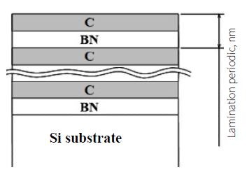
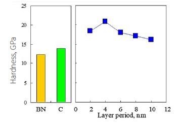
To enhance carbon film strength, elements like boron (B) and nitrogen (N), which form strong bonds with carbon (C), come into play. Nano-periodic lamination involves stacking different materials alternately at the nanometer scale, resulting in energy changes within the film due to its nano-periodic structure. This design leads to improved properties like elasticity and hardness more than the single films of the constituent materials stacked individually (Figure 9).
During nanoindentation using a diamond probe with varying nano-periods (2, 4, 6, 8, and 10 nm), the 4 nm-period film emerged as the hardest (Figure 10). Moreover, the laminated film exhibited greater hardness than the individual C and BN films.
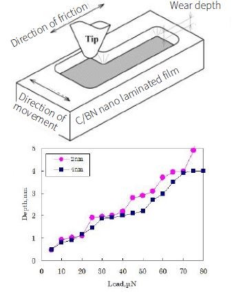
The laminated film's outstanding tribology characteristics make it versatile as a thin film, with potential applications in various areas. For instance, it can serve as an AFM high-density recording medium. Leveraging the laminated film, precise layer-by-layer removal can be achieved, enabling accurate processing to a specific depth.
laminated film
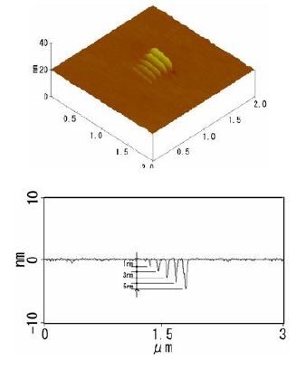
Figures 11 and 12 illustrate step groove processing using a C/BN 2 nm periodic laminated film, designed for multi-value recording at the same location. The processing parameters involve a 200 nm processing length and a 100 nm line interval. The initial processing depth was 1 nm, increasing by 1 nm with each subsequent process, culminating in 5 nm for the fifth iteration. This demonstrates the adjustability of the processing depth based on the number of processing cycles.
BN laminated film by AFM
laminated film
Moving forward, we explore an instance of silicon nanomachining. Employing atomic-order processing, nanolithography is harnessed to create nanomachines and nanodevices [6]. An additional advantage of this method is that the machined topography can be measured at the nanometer scale using the same chip post-nanomachining.
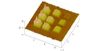
Figure 13 shows an example of the nano rise topography formed by the AFM. The load was increased from 10 μN in the upper right to 10 μN each, 20 μN, 30 μN in the center, and to 90 μN in the lower left. Although the height of the bumps increases with the load, the bumps [7] have almost the same shape.
The observed bulging phenomenon is attributed to the friction of the diamond indenter, causing bond breakage at areas of maximum shear or tensile stress within the silicon. These areas react with water or oxygen from the surface and surroundings to form silicon oxide and silicon hydroxide [8,9].
Conclusion
Atomic Force Microscopy (AFM) has revolutionized the realm of nanoscale analysis through its versatile techniques. Technique A, focused on Property Mapping, enables the simultaneous evaluation of topography, surface potential, and magnetic force of complex materials, shedding light on intricate material characteristics that would be difficult to discern through topography alone. Technique B, nanomechanical characterization, empowers precise assessment of elasticity, adhesion, and deformation through the innovative PinPoint nanomechanical mode. This technique offers a comprehensive understanding of materials' mechanical properties, aiding advancements in material science. Technique C, thin film characterization and nanofabrication, propels thin film analysis to new heights, revealing novel insights into mechanical properties and paving the way for atomic-level processing techniques. Collectively, these techniques broaden our horizons in material research, offering unprecedented insights into the atomic world and sparking transformative possibilities in fields ranging from electronics to materials engineering. The dynamic synergy of these techniques positions AFM as an invaluable tool driving innovation and discovery across diverse scientific domains.
References
[1] Sample courtesy: Hyun-Bae Lee, Nuclear & Quantum Engineering, KAIST, Korea
[2] Park Systems Introduces PinPoint™ Nanomechanical Mode to Characterize Nano Mechanical Properties of Materials and Biological Cells. Available from: http:// www.parkafm.com/index.php/company/news/pressrelease/ 450-nanomechanical
[3] Research Application Technology Center, Park Systems Corp: Quantitative frictional properties measurement using atomic force microscopy (2021)
[4] 三宅正二郎,関根幸男、金 鍾得、山本洋和、 ナノ周期 積層膜の摩耗特性を活用したナノ加工技術の開発、 精密 工学会誌、 66、12 (2000) 1958
[5] Shojiro MIYAKE and Jongduk KIM, “Nanoprocessing of Carbon and Boron Nitride Nanoperiod Multilayer Films”, Jpn. J. Appl. Phys. Vol. 42 (2003) pp. L 322–L 325.
[6] 金 鍾得、三宅正二郎、 メカノケミカル反応によるシ リコンのナノメータ隆起・ 除去加工とそのエッチングマス クへの応用、精密工学会誌、 68、5(2002)695
[7] Shojiro Miyake,Mei Wang and Jongduk Kim “Silicon Nanofabrication by Atomic Force Microscopy-Based Mechanical Processing”, Journal of Nanotechnology 2014 1-19
[8] Shojiro Miyake and Jongduk Kim, “Increase and decrease of etching rate of silicon due to diamond tip sliding by changing scanning density”, Japanese Journal of Applied Physics, vol. 41, no. 10, pp. L1116–L1119, 2002
[9] Shojiro Miyake and Jongduk Kim, “Nanoprocessing of silicon by mechanochemical reaction using atomic force microscopy and additional potassium hydroxide solution etching”, Nanotechnology, vol. 16, no. 1, pp. 149–157, 2005.